CVA6 Requirement Specification
Editor: Jerome Quevremont
Revision 1.0.1
License
Copyright 2022 OpenHW Group and Thales Copyright 2018 ETH Zürich and University of Bologna
SPDX-License-Identifier: Apache-2.0 WITH SHL-2.1
Licensed under the Solderpad Hardware License v 2.1 (the “License”); you may not use this file except in compliance with the License, or, at your option, the Apache License version 2.0. You may obtain a copy of the License at https://solderpad.org/licenses/SHL-2.1/. Unless required by applicable law or agreed to in writing, any work distributed under the License is distributed on an “AS IS” BASIS, WITHOUT WARRANTIES OR CONDITIONS OF ANY KIND, either express or implied. See the License for the specific language governing permissions and limitations under the License.
Introduction
CVA6 is a RISC-V compatible application processor core that can be configured as a 32- or 64-bit core (RV32 or RV64). It includes L1 caches, optional MMU, optional PMP and optional FPU.
It is an industrial evolution of ARIANE created by ETH Zürich and the University of Bologna. It is written in SystemVerilog and maintained by the OpenHW Group.
This specification is organized as requirements that apply to the “Scope of the IP”.
The requirement list is to be approved by the OpenHW Group Technical Work Group (TWG), as well as its change requests.
The specification will be complemented by a user’s guide.
Revision 1.0.0 refers to the product of the first CVA6 project led at OpenHW Group. It is a placeholder in case of future evolutions after project freeze (PF gate).
A list of abbreviations is available at the end of this document.
Scope
Scope of the IP
The scope of the IP is the subsystem that is specified below and that will undergo verification with a 100% coverage goal. In the verification plans, the scope of the IP can be broken down in several DUT (design under test).
The scope of the IP is the CVA6 hardware supporting all the features used in products based on CVA6.
CVA6 exists in two main configurations: CV64A6 and CV32A6. A requirement referring to CVA6 applies to both configurations.
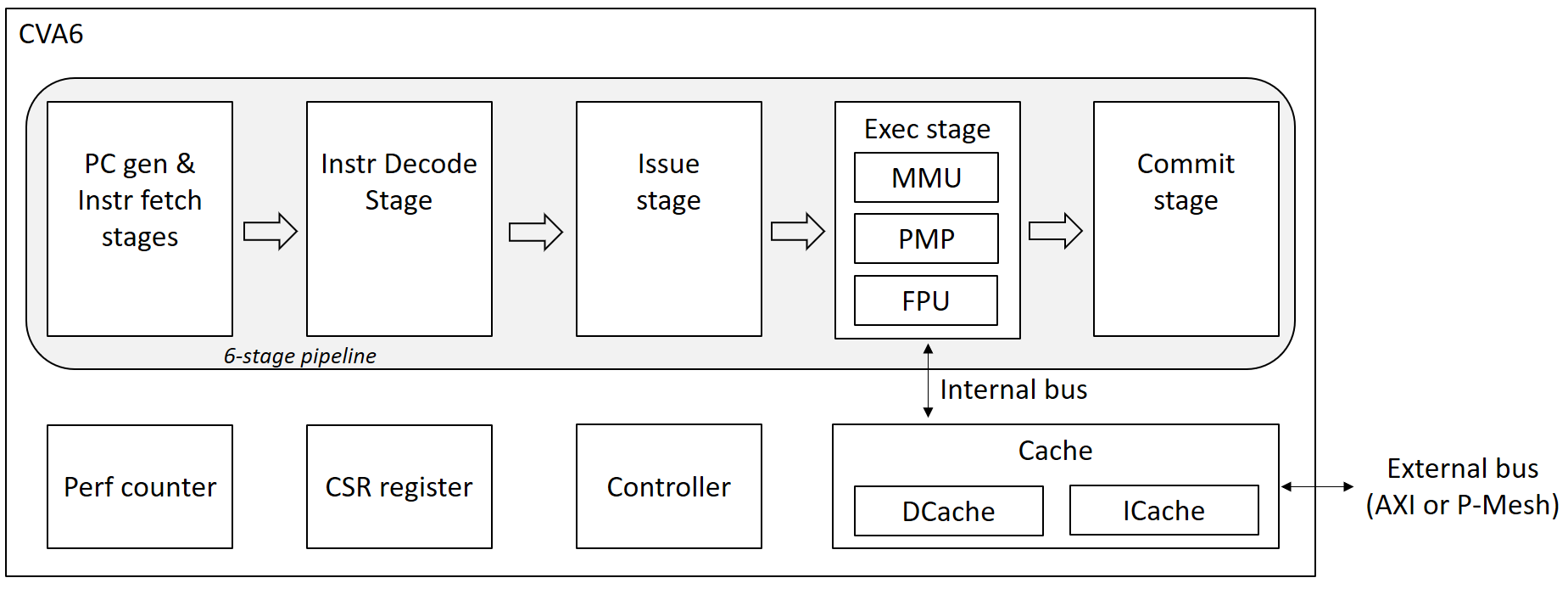
As displayed in the picture above, the IP comprises:
The CVA6 core;
L1 write-through cache;
Optional FPU;
Optional MMU;
Optional PMP;
CSR;
Performance counters;
AXI interface;
Interface with the P-Mesh coherence system of OpenPiton.
These are not part of the IP (several solutions can be used):
CLINT or PLIC Interrupt modules;
Debug module (such as DTM);
Support of L1 write-back cache (this might come later as an update).
In addition to these main configurations, several fine grain parameters are available.
Unless otherwise stated, an optional feature is controlled by a SystemVerilog parameter. If not selected, the optional feature will not be present in the netlist after synthesis.
The reader’s attention is drawn to the difference between an optional feature (“…shall support as an option…”) and a desired goal (“…should support…”, “…should reduce latency…”).
These are not in the scope of this specification:
SW layers, such as compiler and OSes (that can however be part of the OpenHW Group CVA6 project);
SW emulation of RISC-V optional extensions ( feasible but the scope of the IP is the core hardware);
Other features included in the testbench (main memory, firmware, interconnect…), the verification coverage of which will not be measured;
The vector coprocessor (CV-VEC) that is planned to interface with CV64A6.
Initial Release
The CVA6 is highly configurable via SystemVerilog parameters. It is not practical to fully document and verify all possible combinations of parameters, so a set of “viable IP configurations” has been defined. The full list of parameters for this configuration will be detailed in the users’ guide.
Below are the configuration of the first releases of the CVA6.
Release ID |
Target |
ISA (main ext.) |
XLEN |
FPU |
CV-X-IF |
MMU |
L1 D$ |
L1 I$ |
|---|---|---|---|---|---|---|---|---|
|
ASIC |
IMC |
32 |
No |
Yes |
None |
(2 kB) |
(2 kB) |
|
ASIC |
IMC |
32 |
No |
Yes |
Sv32 |
16kB |
16 kB |
|
ASIC |
IMACFDB |
64 |
Yes |
Yes |
Sv39 |
32kB |
32 kB |
Note for CV32A60X: Its first industrial use is without caches. Therefore its cache size is not representative.
References
Applicable specifications
To ease the reading, the reference to these specifications can be implicit in the requirements below. For the sake of precision, the requirements identify the versions of RISC-V extensions from these specifications.
[RVunpriv] “The RISC-V Instruction Set Manual, Volume I: User-Level ISA, Document Version 20191213”, Editors Andrew Waterman and Krste Asanović, RISC-V Foundation, December 13, 2019.
[RVpriv] “The RISC-V Instruction Set Manual, Volume II: Privileged Architecture, Document Version 20211203”, Editors Andrew Waterman, Krste Asanović and John Hauser, RISC-V Foundation, December 4, 2021.
[RVdbg] “RISC-V External Debug Support, Document Version 0.13.2”, Editors Tim Newsome and Megan Wachs, RISC-V Foundation, March 22, 2019.
[RVZc] “RISC-V Zc* Code Size Reduction v1.0”, Editor Tariq Kurd, Codasip, April, 2023. https://wiki.riscv.org/display/HOME/Recently+Ratified+Extensions
[RVcompat] “RISC-V Architectural Compatibility Test Framework”, https://github.com/riscv-non-isa/riscv-arch-test.
[AXI] AXI Specification, https://developer.arm.com/documentation/ihi0022/hc.
[CV-X-IF] “OpenHW Group Specification: Core-V eXtension interface (CV-X-IF)”, version 1.0.0, https://docs.openhwgroup.org/projects/openhw-group-core-v-xif/.
[OpenPiton] “OpenPiton Microarchitecture Specification”, Princeton University, https://parallel.princeton.edu/openpiton/docs/micro_arch.pdf.
Reference documents
[RVcmo] “RISC-V Base Cache Management Operation ISA Extensions, version 1.0-fd39d01, 2022-01-12”
[CLINT] Core-Local Interruptor (CLINT), “SiFive E31 Core Complex Manual v2p0”, chapter 6, https://static.dev.sifive.com/SiFive-E31-Manual-v2p0.pdf
Functional requirements
General requirement
GEN‑10 |
CVA6 shall be fully compliant with RISC-V specifications [RVunpriv], [RVpriv] and [RVdbg] by implementing all mandatory features for the set of extensions that are selected and by passing [RVcompat] compatibility tests. |
As the RISC-V specification leaves space for variations, this specification specifies some of these variations.
RISC-V standard instructions
To ease tracing to verification, the extensions have been split in independent requirements.
ISA‑10 |
CV64A6 shall support RV64I base instruction set, version 2.1. |
ISA‑20 |
CV32A6 shall support RV32I base instruction set, version 2.1. |
ISA‑30 |
CVA6 shall support the M extension (integer multiply and divide), version 2.0. |
ISA‑40 |
CVA6 shall support the A extension (atomic instructions), version 2.1. |
ISA‑50 |
CV32A6 shall support as an option the F extension (single-precision floating-point), version 2.2. |
ISA‑60 |
CV64A6 shall support as an option the F and D extensions (single- and double-precision floating-point), version 2.2. |
ISA‑70 |
CV64A6 shall support as an option the F extension (single-precision without double-precision floating-point), version 2.2. |
ISA‑80 |
CVA6 shall support as an option the C extension (compressed instructions), version 2.0. |
ISA‑90 |
CVA6 shall support the Zicsr extension (CSR instructions), version 2.0. |
ISA‑100 |
CVA6 shall support the Zifencei extension, version 2.0. |
ISA-120 |
CVA6 should support as an option the B extension (bit manipulation), version 1.0. The B extension comprises the Zba, Zbb, Zbc and Zbs extensions. |
ISA-130 |
CVA6 should support as an option the Zicond extension (integer conditional operations) version 1.0. |
ISA-140 |
CVA6 should support as an option the Zcb extension version 1.0. |
ISA-150 |
CVA6 should support as an option the Zcmp extension version 1.0. |
ISA-160 |
CVA6 should support as an option the Zcmt extension version 1.0. |
ISA-170 |
CVA6 should support as an option the Zkn extension (NIST algorithm suite). The Zkn extension comprises the Zbkb, Zbkc, Zbkx, Zkne, Zknd and Zknh extensions. |
Note to ISA-60 and ISA-70: CV64A6 cannot support the D extension without the F extension.
Privileges and virtual memory
The MMU includes a TLB and a hardware PTW.
PVL‑10 |
CVA6 shall support machine, supervisor, user and debug privilege modes. |
PVL‑20 |
CV64A6 shall support as an option the Sv39 virtual memory, version 1.11. |
PVL‑30 |
CV32A6 shall support as an option the Sv32 virtual memory version 1.11. |
PVL‑40 |
CVA6 instances that do not feature virtual memory shall support the Bare mode. |
PVL‑50 |
CVA6 shall feature PMP (physical memory protection) as an option. |
PVL‑60 |
CV64A6 shall support as an option the H extension (hypervisor) version 1.0. |
CSR
There are no requirements related to CSR as they derive from other requirements, such as PVL-10, PVL-60… Details of CSRs will be available in the user’s manual.
Performance counters
Performance counters are important features for safety-critical applications.
HPM‑10 |
CVA6 shall implement the 64-bit
|
HPM‑20 |
CVA6 shall implement as an
option six generic 64-bit
performance counters located in
|
HPM‑30 |
Each of the six generic performance counters shall be able to count events from one of these sources:
|
HPM‑40 |
The source of events counted by
the six generic performance
counters shall be selected by the
|
HPM‑50 |
CVA6 shall allow the supervisor
access of performance counters
through enabling of
|
HPM‑60 |
CVA6 shall allow the user access
of performance counters through
enabling of |
HPM‑70 |
CVA6 shall implement the
|
HPM‑80 |
CVA6 shall implement the
read-only |
The user’s manual will detail the list of counters, events and related controls.
Cache requirements
Caches increase the performance of the processor with regard to memory accesses. Most of their added value for the IP is specified through performance requirements in another section. Here below are specific requirements for these caches.
The project would like to adopt the recently ratified [RVcmo] specification. The analysis yet needs to be performed and will likely lead to an evolution of this specification.
L1 write-through data cache
In the requirements below, L1WTD refers to the L1 write-through data cache that is part of the CVA6.
The first two requirements express the write-through feature. Some requirements are useful for security- and safety-critical applications where a high level of timing predictability is needed.
L1W‑10 |
L1WTD shall reflect all write accesses (stores) by the CVA6 core to the external memory within an upper-bounded number of cycles. The upper-bound is fixed but not specified here. |
L1W‑20 |
L1WTD shall not change the order of write accesses to the external memory with respect to the order of write accesses (stores) received from the CVA6 core. |
L1W‑30 |
L1WTD should offer the following size/ways configurations:
|
L1W‑40 |
L1WTD shall support datasize extension to store EDC, ECC or other information. The numbers of bits of the extension is defined by a compile-time parameter. |
L1W‑50 |
To interface with the P-Mesh coherence system of OpenPiton, L1WTD shall have a line invalidate external command that invalidates the content of a line upon request. |
L1W‑60 |
Some physical memory regions shall be configurable as not L1WTD cacheable at design time. |
L1W‑70 |
It shall be possible to
invalidate L1WTD content with the
|
L1W‑80 |
The replacement policy of L1WTD shall be LFSR (pseudo-random) or LRU (least recently used). |
L1W‑90 |
L1WTD should offer a feature to transform cache ways into a scratchpad. Alternatively, this requirement can be realized with a separate scratchpad. |
L1W‑100 |
A custom CSR shall allow to disable or enable L1WTD. |
Cache counters are defined in the performance counters.
32 kbytes & 4 ways is not feasible with the current architecture. Other size/ways configurations may be implemented in the design.
The design will support one replacement policy allowed by L1W-80.
These L1WTD requirements apply to the legacy WT cache from PULP. They also apply to the HPDCache that will supersede the legacy PULP caches. Note that the HPDCache has more features, such as write-back options, that are beyond the scope of this specification.
L1 Instruction cache
In the requirements below, L1I refers to the L1 instruction cache that is part of the CVA6.
Some requirements are useful for security- and safety-critical applications where a high level of timing predictability is needed.
L1I‑10 |
L1I should offer the following size/ways configurations:
|
L1I‑20 |
L1I shall support datasize extension to store EDC, ECC or other information. The numbers of bits of the extension is defined by a compile-time parameter. |
L1I‑30 |
To interface with the P-Mesh coherence system of OpenPiton, L1I shall have a line invalidate external command that invalidates the content of a line upon request. |
L1I‑40 |
It shall be possible to
invalidate L1I content with the
|
L1I‑50 |
The replacement policy of L1I shall be LFSR (pseudo-random) or LRU (least recently used). |
L1I‑60 |
L1I should offer a feature to transform cache ways into a scratchpad. Alternatively, this requirement can be realized with a separate scratchpad. |
L1I‑70 |
A custom CSR shall allow to disable or enable L1I. |
Cache counters are defined in the performance counters section.
32 kbytes & 4 ways is not feasible with the current architecture. Other size/ways configurations may be implemented in the design.
The design will support one replacement policy allowed by L1I-50.
FENCE.T custom instruction
There are discussions within RISC-V International to define a
specification for FENCE.T. The specification below reflects the
situation prior to this RISC-V specification, based on Nils Wistoff’s
work. If a RISC-V specification is ratified, the CVA6 specification will
likely switch to it.
FET‑10 |
CVA6 should support the
|
FET‑20 |
|
FENCE.T goes beyond FENCE and FENCE.I as it clears L1 caches,
TLB, branch predictors… It is a countermeasure for SPECTRE-like
attacks. It is also useful in safety-critical applications to increase
execution time predictability.
It is not yet decided if the FENCE.T instruction arguments can be
used to select a subset of microarchitecture features that will be
cleared. The list of arguments, if any, will be detailed in the user’s
guide.
PPA targets
These PPA targets will likely be updated when performance monitoring is integrated in the continuous integration flow.
PPA‑10 |
CVA6 should be resource-optimized on FPGA and ASIC targets. |
PPA‑20 |
CVA6 should target 3.0 CoreMark/MHz , assuming a sufficiently fast memory hierarchy. |
PPA‑25 |
CVA6 should target as an option 4.5 CoreMark/MHz, assuming a sufficiently fast memory hierarchy. |
PPA‑30 |
CV32A6 should run at more than 150 MHz in the cv32a6_imac_sv32 configuration on Kintex 7 FPGA technology, commercial -2 speed grade. |
PPA‑40 |
CV64A6 should run at more than 900 MHz in the cv64a6_imacfd_sv39 configuration on 28FDSOI technology in the worst case frequency corner with the fastest threshold voltage. |
PPA‑50 |
TBD: Placeholder for single-precision floating performance per MHz. |
PPA‑60 |
TBD: Placeholder for double-precision floating performance per MHz. |
PPA-25 comes with the optional dual-issue feature.
Interface requirements
Memory bus
MEM‑10 |
CVA6 memory interface shall comply with AXI5 specification including the Atomic_Transactions property support as defined in [AXI] section E1.1. |
MEM‑20 |
CVA6 AXI memory interface shall
feature user bit extensions on
the data bus ( |
The interface complies with AXI4. However, Atomic_Transactions is only defined in AXI5. For the sake of clarity, we do not use the AXI5-Lite interface.
Debug
DBG‑10 |
CVA6 shall implement both the Abstracted Command and Execution based features outlined in chapter 4 of [RVdbg]. |
In addition, there can be an external debug module, not in the scope of the IP.
Interrupts
IRQ‑10 |
CVA6 shall implement interrupt handling registers as per the RISC-V privilege specification and interface with a CLINT implementation. |
Coprocessor interface
XIF‑10 |
To extend the supported instructions, CVA6 shall have a coprocessor interface that supports the “Issue”, “Commit” and “Result” interfaces of the [CV-X-IF] specification. |
Multi-core interface
TRI‑10 |
CVA6 shall have the Transaction-Response Interface (TRI) needed to interface with the P-Mesh coherence system of OpenPiton, according to [OpenPiton]. |
Design rules
As different teams have different design rules and to ease the integration in FPGA and ASIC design flows:
RUL‑10 |
CVA6 should have a configurable reset signal: synchronous/asynchronous, active on high or low levels. |
RUL‑20 |
CVA6 shall be a super-synchronous design with a single clock input. |
RUL‑30 |
CVA6 should not include multi-cycle paths. |
RUL‑40 |
CVA6 should not include technology-dependent blocks. |
RUL-50 |
CVA6 should support as an option protection of SRAM against single-event upsets (SEU). |
If technology-dependent blocks are used, e.g. to improve PPA on certain targets, the equivalent technology-independent block should be available. Parameters can be used to select between the implementations.